Parameter
Symbol
CDBD
CDBD
1020-G
1030-G
CDBD
10200-G
Unit
Repetitive peak reverse voltage
Continuous reverse voltage
RMS voltage
Maximum forward voltage
I
F=10.0A
Maxium Forward surge current, 8.3ms
singlehalf sine-wave superimposed on
rate load (JEDEC method)
current
MaximumReverse
VR=VRRM TA=25°C
VR=VRRM
TA=100°C
Page 1
QW-BB033
Chip Schottky Barrier Rectifier
REV:A
Comchip Technology CO., LTD.
VRRM
VR
VRMS
IO
VF
IFSM
IR
RθJc
TJ
20
20
14
40
40
28
60
60
42
10.0
0.75
150
0.5
50
3.0
80
80
56
150
150
105
V
V
V
A
V
A
mA
°C/W
°C
0.55
1.00
Operating temperature
Storage temperature
TSTG
-65 to +175
°C
-55 to +125
-55 to +150
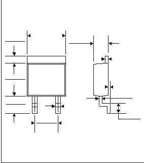
Dimensions
in
inches
and
(
millimeters)
D2PAK
Reverse V
oltage: 20 to 200 Volts
Forward Current: 10.0
Amp
RoHS Device
CDBD1020-G Thru. CDBD10200-G
1040-G
CDBD
1050-G
1060-G
CDBD
CDBD
1080-G
10100-G
CDBD
10150-G
CDBD
50
50
35
J
unction
t
o
C
ase
0.402(10.20)
0.386( 9.80)
0.192(4.8)
0.176(4.4)
0.370(9.40)
0.354(9.00)
0.205(5.20)
0.189(4.80)
0.063(1.60)
0.055(1.40)
0.024(0.60)
0.016(0.40)
0.055(1.40)
0.047(1.20)
0.185(4.70)
0.169(4.30)
0.012(0.30)
0.004(0.10)
0.108(2.70)
0.092(2.30)
0.046(1.20)
0.032(0.80)
30
30
21
100
100
70
CDBD
200
200
140
0.85
IR
mA
2
1
3
Maximum Forward rectified current
(See fig. 1)
Typ.Thermal
resistance
Features
-Batch
process
design, excellent
power
dissipation
offers
better
reverse
leakage current
and
thermal
resistance.
-Low
profile
surface
mounted
application
in
order
to
optimize
board
space.
-Low
power
loss, high
efficiency.
-High
current
capability, low
forward
voltage
drop.
-High
surge
capability.
-Guarding
for
overvoltage
protection.
-Ultra
high-speed
switching.
-Silicon
epitaxial
planar
chip, metal
silicon
junction.
-Lead-free
part meets
environmental
standards
of
MIL-STD-19500 /228
Mechanical data
-Case: TO-263/D2PAK, molded plastic.
-Terminals: solderable per MIL-STD-750,
method 2026.
-Polarity: Indicated by cathode band.
-Weight:1.70 gram(approx.).
-Weunting Position: Any
PIN
1
PIN
3
PIN
2
Maximum Ratings
(At Ta=25°C, unless otherwise noted)


发布紧急采购,3分钟左右您将得到回复。
相关PDF资料
CDBD10200-G
DIODE SCHOTTKY 200V 10A D2PAK
CDBD20100-G
DIODE SCHOTTKY 100V 20A D2PAK
CDBD20200-G
DIODE SCHOTTKY 200V 20A D2PAK
CDBD20200-HF
DIODE SCHOTTKY 200V 20A D2PAK
CDBH3-54C-G
DIODE SCHOTTKY 30V 200MA SOT523
CDBH3-54S-G
DIODE SCHOTTKY 30V 200MA SOT523
CDBV3-00340C-G
DIODE SCHOTTKY 40V 30MA SOT323
CDBV6-54BR-G
DIODE SCHOTTKY 30V 0.2A SOT-363
相关代理商/技术参数
CDBD10100-HF
制造商:COMCHIP 制造商全称:Comchip Technology 功能描述:Chip Schottky Barrier Rectifier
CDBD10150-G
功能描述:肖特基二极管与整流器 VR=150V IO=10A RoHS:否 制造商:Skyworks Solutions, Inc. 产品:Schottky Diodes 峰值反向电压:2 V 正向连续电流:50 mA 最大浪涌电流: 配置:Crossover Quad 恢复时间: 正向电压下降:370 mV 最大反向漏泄电流: 最大功率耗散:75 mW 工作温度范围:- 65 C to + 150 C 安装风格:SMD/SMT 封装 / 箱体:SOT-143 封装:Reel
CDBD10150-HF
制造商:COMCHIP 制造商全称:Comchip Technology 功能描述:Chip Schottky Barrier Rectifier
CDBD10200-G
功能描述:肖特基二极管与整流器 VR=200V IO=10A RoHS:否 制造商:Skyworks Solutions, Inc. 产品:Schottky Diodes 峰值反向电压:2 V 正向连续电流:50 mA 最大浪涌电流: 配置:Crossover Quad 恢复时间: 正向电压下降:370 mV 最大反向漏泄电流: 最大功率耗散:75 mW 工作温度范围:- 65 C to + 150 C 安装风格:SMD/SMT 封装 / 箱体:SOT-143 封装:Reel
CDBD10200-HF
制造商:COMCHIP 制造商全称:Comchip Technology 功能描述:Chip Schottky Barrier Rectifier
CDBD1020-G
制造商:COMCHIP 制造商全称:Comchip Technology 功能描述:Chip Schottky Barrier Rectifier
CDBD1020-HF
制造商:COMCHIP 制造商全称:Comchip Technology 功能描述:Chip Schottky Barrier Rectifier
CDBD1030-G
制造商:COMCHIP 制造商全称:Comchip Technology 功能描述:Chip Schottky Barrier Rectifier
